

一、生成物情況
1、物品的特點:
- 進入電阻整體規模:3.0V-32V
- 發送端電壓企業規模:2.0V-30V
- 可程序語言轉換開關谷值電流量:20A
- 觸點開關周期:150KHz/300KHz
- 集玉成快充和談、buck-boost充擊穿放肆器、交流電源途經辦理好
- 撐持A+C利于、集合I2C通信技術
- 容量電池充電實例3V-4.5V可每10mV累加設置,撐持1-6串容量電池充電
- 匹配器防拉死電阻值VINREG可每10mV遞加小編
- 填寫填寫電流值限量可每10mA依次增加編輯器
- 輸入直流電壓可每10mV遞加剪輯
- 撐持欠壓、過壓、過流、不導通、工作溫度等擋拆
- 集成式LDO
- 封裝類型:QFN5x5-40
2、采用大道理圖:
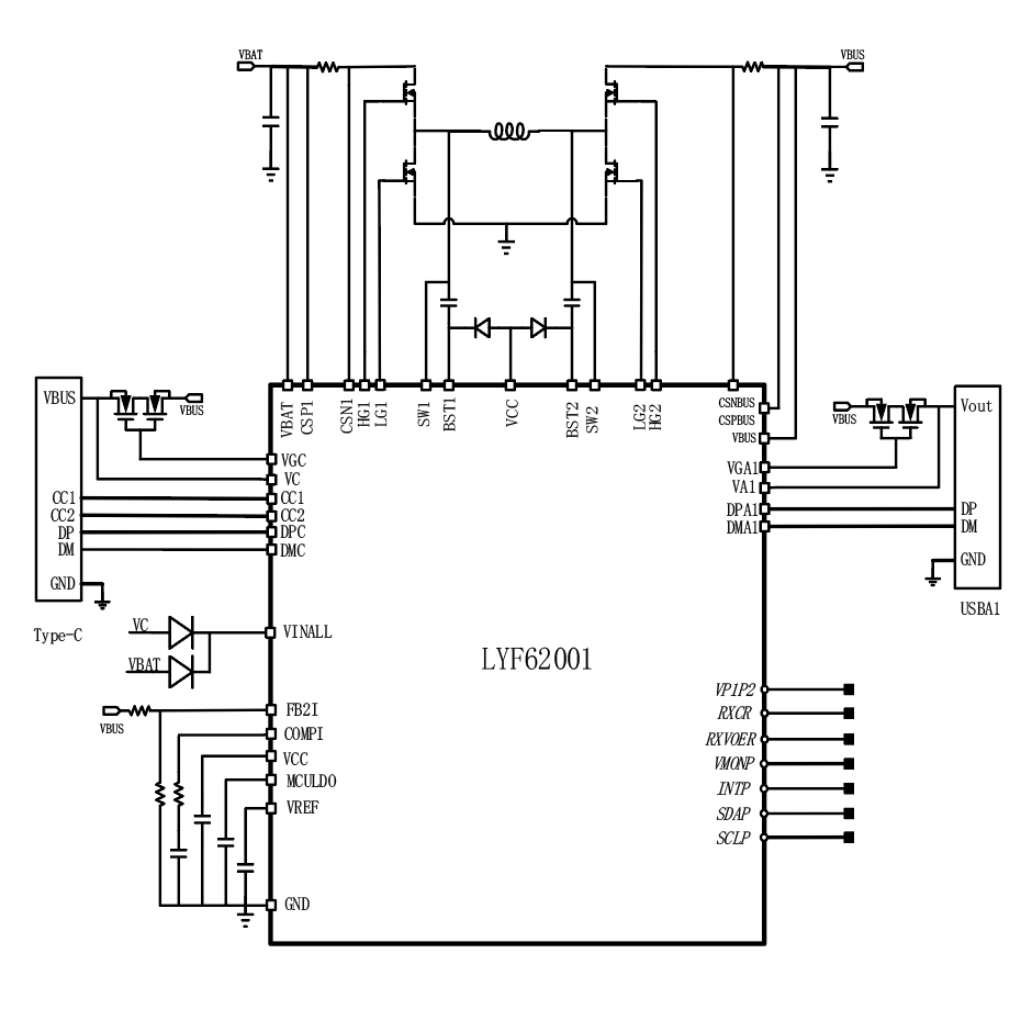
LYF62001利用道理圖
3、代謝物描寫出
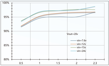
LYF62001 is a high efficiency, synchronous bi-directional buck-boost charger with integrated fast charge protocols. It is a comprehensive and flexible buck-boost charger platform designed for most of fast charging applications with type-C port and PD protocol. It can be programmed to buck charging, boost charging or buck-boost charging. LYF62001 provides I2C interface to communicate with MCU, provides high voltage sensing for battery and BUS terminals, accurate rail-rail current sensing for battery current, BUS current and USB ports currents. It also provides high voltage blocking for CC1, CC2, DP, DM communication signals for all of the USB ports. LYF62001 can work with a general MCU to provide a complete, powerful and flexible buck-boost charging system for all kinds of fast charge application such as power bank, battery packs, or portable energy cubic etc. In charging mode, it steps up or down the input voltage to effectively charge the batteries. LYF62001 supports trickle charging, constant current (CC) charging and constant voltage (CV) charging management. The charging current and charging voltage can be programmed by two 12-bit DAC converters. The LYF62001 features I2C interface, so the user can easily control the charging/discharging mode, and program charging current, charging voltage, output voltage, and output current limits through I2C. It also monitors the status of USB ports and provides two NMOS gate drivers to control the power path independently. User can also use I2C to monitor the status of DC-DC, even the whole system. LYF62001 also provides VMON pin, through which the MCU can monitor VBUS, VBAT voltage, IBUS, IBAT current and the current of each port in real time. All these features simplify the system design and reduce BOM cost for any charging system.The LYF62001 supports under voltage protection, over voltage protection, over current protection, short circuit protection and over temperature protections to ensure system safety under different abnormal conditions.
4、杰出典范應用處景
- 專研寶
- 挪動微電網
- 電池板包
- 挪動裝置(如電開小東西、肌肉筋膜槍、挪動廚房電器等)
- 應對啟動的開關電源
- 智力USB插板
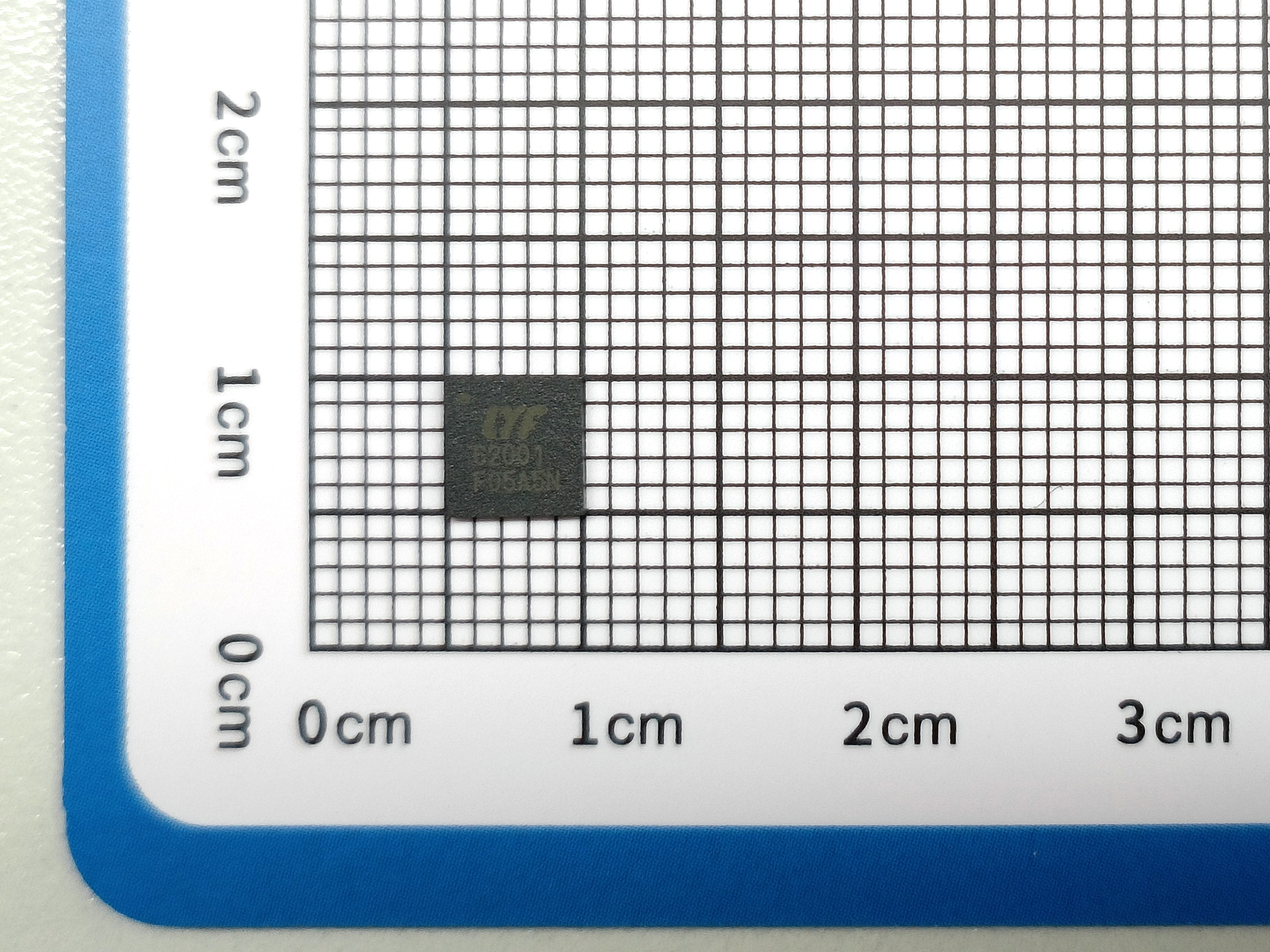
5、打包封裝相關信息
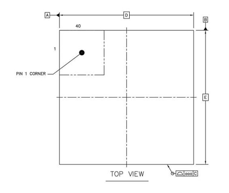
LYF62001頂視圖
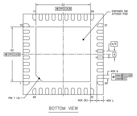
LYF62001背視圖
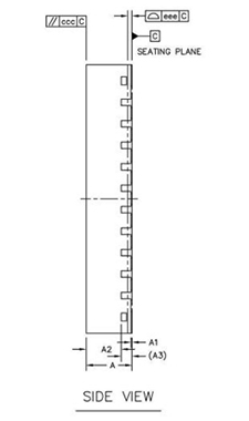
LYF62001側視圖
6、管腳界說和功較描寫出
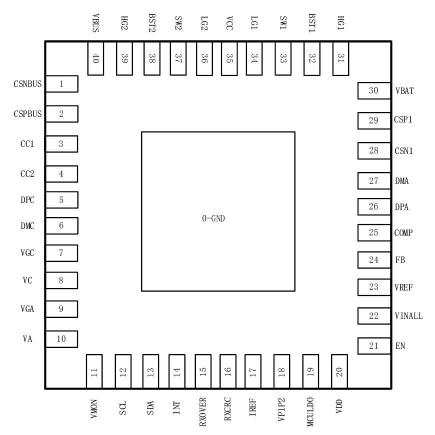
LYF62001管腳界說圖
管腳效果描定
| 序號 | 稱號 | 描寫 |
|---|---|---|
| 1 | CSNBUS | Negative input of a current sense amplifier. Connect to one terminal of the current sense resistor. |
| 2 | CSPBUS | Positive input of a current sense amplifier. Connect to one terminal of the current sense resistor. |
| 3 | CC1 | Configuration Channel 1 for C port |
| 4 | CC2 | Configuration Channel 2 for C port |
| 5 | DPC | D+ signal for C port |
| 6 | DMC | D- signal for C port |
| 7 | VGC | NMOS gate driver to control the external NMOS of C port |
| 8 | VC | Used to sense the voltage of C port. |
| 9 | VGA | NMOS gate driver to control the external NMOS of A port |
| 10 | VA | Used to sense the voltage of A port. |
| 11 | VMON | Used to detect VBUS/VBAT voltage, IBUS/IBAT current, and the voltage drop of cut-off MOS for A/C ports. Connect this pin to MCU with a RC filter. |
| 12 | SCL | I2C clock line. Connect with a pull up resistor (typical 10kΩ). Connect to MCU |
| 13 | SDA | I2C data line. Connect with a pull up resistor (typical 10kΩ). Connect to MCU |
| 14 | INT | Open drain output for interrupt signal. Connect to MCU |
| 15 | RXOVER | Connect this pin to MCU |
| 16 | RXCRC | Connect this pin to MCU |
| 17 | IREF | Reference voltage for input and output current limiting loop. |
| 18 | VP1P2 | 1.2V power supply. |
| 19 | MCULDO | 3.3V voltage output for MCU |
| 20 | VDD | Output of internal 5V linear regulator. Connect a 1μF capacitor from VDD pin to GND as close to the IC as possible. |
| 21 | EN | Logic High will enable the converter. Logic Low will disable the whole LYF62001. EN is pulled high internally by a 5000kΩ resistor. |
| 22 | VINALL | Power supply to the IC. Connect to power rails with low voltage schottky diodes. Place a 1μF capacitor from this pin to GND as close to the IC as possible. |
| 23 | VREF | Reference voltage for voltage control loop |
| 24 | FB | VBUS voltage feedback. |
| 25 | COMP | Error amplifier output and input to the PWM comparator. Connect frequency compensation components to this pin. |
| 26 | DPA | D+ signal for A port |
| 27 | DMA | D- signal for A port |
| 28 | CSN1 | Negative input of a current sense amplifier. Connect to one terminal of the current sense resistor in the VBAT side. |
| 29 | CSP1 | Positive input of a current sense amplifier. Connect to one terminal of the current sense resistor in the VBAT side. |
| 30 | VBAT | Battery voltage or Input voltage. Place a 1μF capacitor from this pin to GND as close to the IC as possible. |
| 31 | HG1 | High side gate driver of switch MOS |
| 32 | BST1 | Boot-Strap pin Connect a 0.1μF or greater capacitor between SW and BST to power the high side gate driver. |
| 33 | SW1 | Power Switching pin. Connect this pin to the switching node of inductor. |
| 34 | LG1 | Low side gate driver of switch MOS |
| 35 | VCC | Power supply for high side and low side driver |
| 36 | LG2 | Low side gate driver of switch MOS |
| 37 | SW2 | Power Switching pin. Connect this pin to the switching node of inductor. |
| 38 | BST2 | Boot-Strap pin Connect a 0.1μF or greater capacitor between SW and BST to power the high side gate driver. |
| 39 | HG2 | High side gate driver of switch MOS. |
| 40 | VBUS | Power node of the charger. |
二、匠人word文件
| 范例 | 標題 | 上傳時候 | 文檔下載 |
| 產品金橋銅業跨接線的截面積大小書(英文翻譯) | LYF62001_Datasheet_en_R1.0 | 2025/04/09 | PDF下載 |
| 設想指南 | LYF62001 PCB設想指南 | 2025/04/09 | PDF下載 |
三、充分利用籌劃
| 序號 | 標題 |
| 1 |
30-100W電開東西充電計劃
30-100W電開東西充電計劃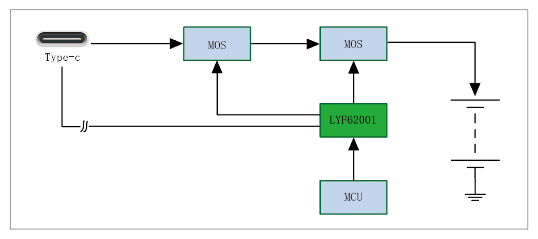
|
| 2 |
儲能電源利用計劃
儲能電源利用計劃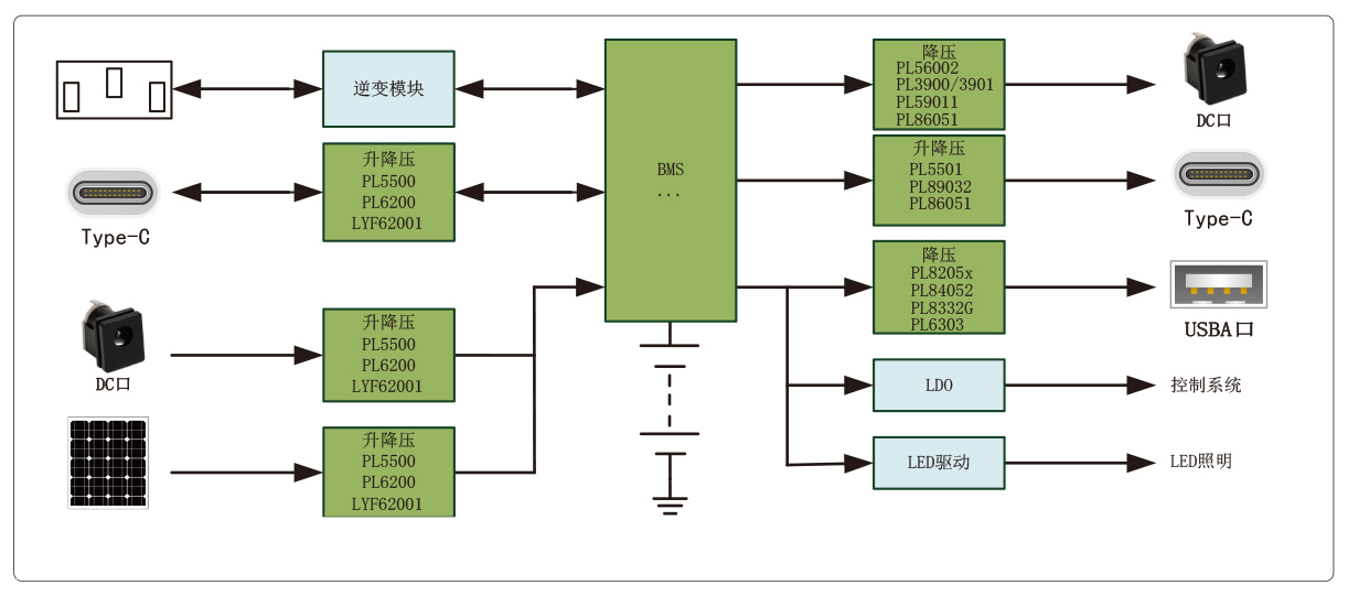
|
| 3 |
充電寶A+C利用計劃
充電寶A+C利用計劃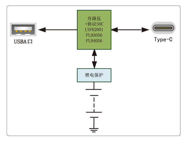
|